(in Cell Reports Physical Science)
- Share
- Share on Facebook
- Share on LinkedIn
Research
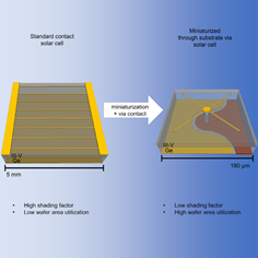
This work by de Lafontaine et al. issued from a collaboration between the LN2/3IT laboratory in Sherbrooke Canada and LTM/CNRS in Grenoble France reports a method to fabricate 3D interconnects on III-V semiconductor devices. A proof of concept is realized on III-V/Ge triple junction solar cells with an area 3 orders of magnitude smaller compared with standard chips. This strategy enables device miniaturization with increased wafer area use.
M. de Lafontaine, T. Bidaud, G. Gay, E.Pargon, C. Petit-Etienne, A. Turala, R. Stricher, S. Ecoffey, M. Volatier, A. Jaouad, C. E. Valdivia, K. Hinzerd, S.Fafard, V. Aimez, M. Darnon, Cell Reports Physical Science 4, 101701, https://doi.org/10.1016/j.xcrp.2023.101701
- Share
- Share on Facebook
- Share on LinkedIn