- Share
- Share on Facebook
- Share on LinkedIn
The emerging electric vehicle market, for example, requires electronic components capable of operating in a hostile environment that can involve high temperatures and high voltages.
For several years now, gallium nitride (GaN) has been receiving particular attention, as it enables the design of so-called power transistors that can operate at very high voltage, high frequency and high temperature.
However, the performance achieved by these devices falls far short of expected specifications. One of the major challenges is to achieve an excellent interface between the transistor gate dielectric and the GaN. Both the choice of dielectric and the conditions under which it is deposited will have a major impact on the transistor's electrical characteristics.
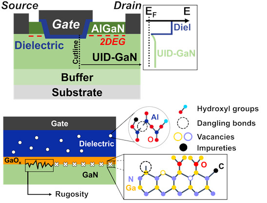
Fig. 1. Schematic representation of a MOSc-HEMT and the interface dielectric/GaN.
At LTM, in close collaboration with CEA-Leti and ST Microelectronics, we develop a building blocks based on a Metal-Isolant-GaN stack, enabling us to study the behavior of dielectrics and the dielectric/GaN interface (fig.1) , and thus suggest ways of improving transistors.
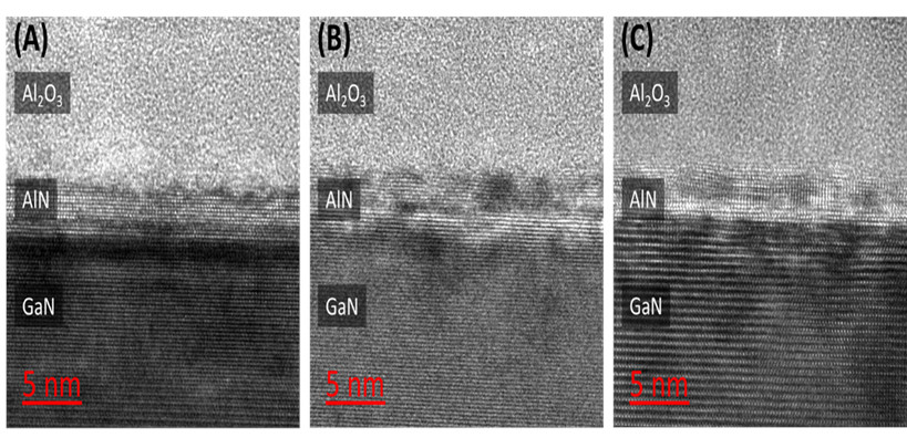
Fig. 2. HRTEM imaging of Al2O3/AlN bilayer with AlN deposited with a substrate bias of A) 0 W, B) 5 W, and C) 10 W.
In addition, angular XPS, AFM, FIB-STEM and TEM measurements are carried out in collaboration with the CEA Leti (fig.2).
Contact : bassem.salem cea.fr (bassem[dot]salem[at]cea[dot]fr)
- Share
- Share on Facebook
- Share on LinkedIn