Postdoctoral position LTM/CNRS (M/F)
- Share
- Share on Facebook
- Share on X
- Share on LinkedIn
Job description / Employment
Key words : Plasma etching process, nitride semiconductor (AlN, AlGaN, GaN), cathodoluminescence, MOVPE process, core-shell architecture, betavoltaic source.
CONTEXT
Beta voltaic (BV) sources harness the energy produced by the radioactive decay of beta particles to generate electricity. They are made from a p-i-n structure equivalent to a photovoltaic cell, except that it is beta radiation (high-energy electrons resulting from the disintegration of neutrons into protons), and not photons from the solar spectrum, that are absorbed by the p-i-n junction and then converted into electrical energy. Unlike traditional chemical batteries, these generators have an exceptional lifespan, reaching several decades without recharging, due to the long half-life of the isotopes used, such as tritium or nickel-63. Their small size, maintenance-free operation and ability to provide stable, continuous power make them particularly attractive for critical applications such as medical implants (pacemakers), satellites, drones and on-board sensors in extreme environments. Although betavoltaic technology is very promising, it has not yet been mastered, and total power conversion efficiency does not exceed 5% [1].
The ANR Nobel project, which brings together 4 partners (LTM/CNRS, pheliqs/CEA, Institut Néel/CNRS and CREAH/CNRS), is proposing a new beta voltaic battery architecture based on wide bandwidth p-i-n junctions using nitride semiconductor core-shell nanowires (GaN, AlN, AlGaN), in order to overcome the efficiency limitations inherent in the planar architectures of current cells.(see Figure 1)
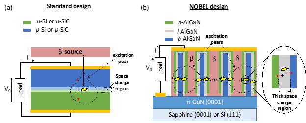
Figure 1: (a) Conventional planar architecture of a BV battery. (b) 3D architecture proposed by the NOBEL project.
In this context, the aim of the postdoctoral project is to develop and characterise plasma etching and wet etching processes for high form factor AlGaN and GaN wires, which constitute the first technological stage in the manufacture of betavoltaic sources.These wires will be used by the project partners to grow quantum wells in core-shell architecture in order to produce p-i-n junctions.
[1] C. Zhou et al., “Review—Betavoltaic Cell: The Past, Present, and Future”, ECS J. Solid State Sci. Technol., 10, 027005, (2021). doi: 10.1149/2162-8777/abe423.
TASK
The work required as part of this postdoc is to
1) Develop plasma etching processes for AlGaN and GaN wires with a high form factor
2) Develop KOH-based wet treatments to restore the etched wire surfaces
3) Characterise the processes morphologically (SEM, FIB-STEM, AFM), chemically (XPS) and optically (cathodoluminescence).
Download
profil postdoc gravure Nobel_ EN.pdf (PDF, 858.89 KB)
profil postdoc gravure Nobel_ FR.pdf (PDF, 863.53 KB)
- Share
- Share on Facebook
- Share on X
- Share on LinkedIn