- Share
- Share on Facebook
- Share on LinkedIn
The perpetual increase in complexity of the stacks and architectures of advanced CMOS devices is challenging conventional plasma technologies based on low-pressure inductively coupled (ICP) or capacitively coupled (CCP) reactors. These approaches show intrinsic limitations when it comes to structuring matter with nanometric or even atomic precision. This is why the Advanced Plasma Processing group of PROSPECT, in close partnership with the equipment manufacturer AMAT, is committed to proposing innovative etching concepts and developing breakthrough plasma technologies to structure matter ever more finely. Thanks to successive renewals of our collaboration agreements with AMAT, the etching reactors of the 300 mm platform are continuously upgraded with the manufacturer’s latest technological advances.
In recent years, the Advanced Plasma Processing group has been working on two technologies:
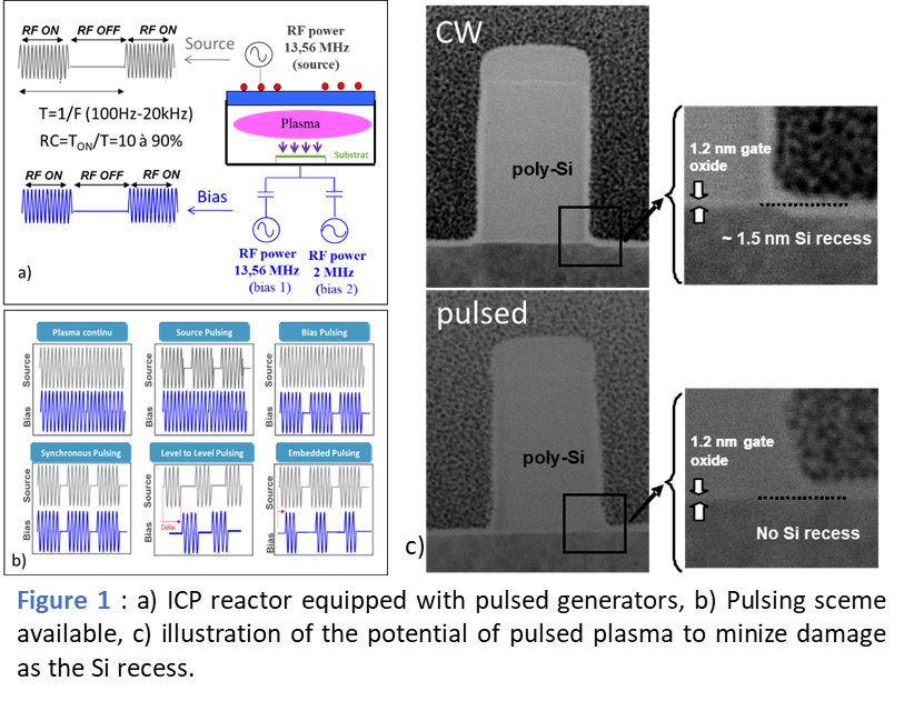
1) Pulsed plasma technologies
The two ICP reactors of the 300 mm etching platform are equipped with generators that allow short-pulse modulation of both the RF power injected into the plasma and the RF bias power applied to the substrate. The modulation of the two generators can be independent, synchronized, and more recently asynchronized (see Fig. 1a,b). This reactor evolution enables precise, quasi-independent, time-resolved control of all plasma parameters governing plasma–surface interactions: the ion flux and energy, and the chemical nature of the plasma species.
Over the past 20 years, the team has clearly demonstrated the potential of pulsed plasma technologies to improve process control at the nanometric scale and to minimize plasma-induced damage (see Fig. 1c) [1–9]. The study of the mechanisms involved in pulsed plasmas will continue in order to address ever more complex challenges associated with the miniaturization of CMOS devices at sub-5 nm technology nodes.
2) An innovative etching concept: the Smart etch
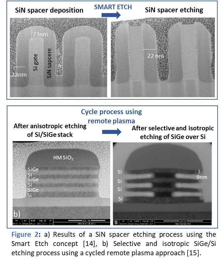
In recent years, the group has worked on a new etching concept, called Smart Etch [10], which consists of cycling light-ion implantation steps carried out using a capacitive plasma, with selective removal steps driven by neutrals produced in a remote plasma. This approach enables quasi “atomic layer by atomic layer” etching (quasi-ALE, for Atomic Layer Etching).
This concept has demonstrated its potential for performing selective anisotropic etching (for example, the etching of SiN spacers in a transistor gate, a process that selectively removes the horizontal surfaces of SiN relative to the vertical surfaces with nanometric precision, (Fig. 2a) [11–14], as well as selective isotropic etching (Fig. 2b) (for example, for the fabrication of horizontal Si nanowires in gate-all-around devices, where a two-step cycled process using only remote plasmas enabled the selective removal of SiGe with respect to Si) [15].
Bibliography
-
Pulsed high-density plasmas for advanced dry etching processes, S. Banna et al, J. Vac. Sci. Technol. A 30, 040801 (2012).<10.1116/1.4716176>
-
Reducing damage to Si substrates during gate etching processes by synchronous plasma pulsing, C. Petit-Etienne et al., J. Vac. Sci. Technol. B 28, 926-935 (2010) <10.1116/1.3483165>
-
Atomic-scale silicon etching control using pulsed Cl2 plasma , C. Petit-Etienne et al.J. Vac. Sci. Technol. B 31, 011201 (2013) <10.1116/1.4768717>
-
Silicon recess minimization during gate patterning using synchronous plasma pulsing, C. Petit-Etienne et al, J. Vac. Sci. Technol. B 30, 040604 (2012) <10.1116/1.4737125>
-
Ion flux and ion distribution function measurements in synchronously pulsed inductively coupled plasmas, M. Brihoum, G. Cunge, M. Darnon, D. Gahan, O. Joubert, N. S-J. Braithwaite, J. Vac. Sci. Technol. A 31(2), 020604 (2013), <10.1116/1.4790364>
-
Atomic-scale silicon etching control using pulsed Cl2 plasma, C. Petit-Etienne, M. Darnon, P. Bodart, M. Fouchier, G. Cunge, E. Pargon, L. Vallier, O. Joubert and S. Banna, J. Vac. Sci. Technol. B 31, 011201 (2013); <10.1116/1.4768717>
-
Sidewall passivation layer thickness and composition profiles of etched silicon patterns from angle resolved x-ray photoelectron spectroscopy analysis, M.Haass, M. Darnon, O. Joubert, J. Appl. Phys. 111, 124905 (2012); <10.1063/1.4729775>
-
Analysis of pulsed high-density HBr and Cl2 plasmas: Impact of the pulsing parameters on the radical densities, P. Bodart, M. Brihoum, G. Cunge, O. Joubert and N. Sadeghi, J. Appl. Phys., 110 (11), sept. 2011, <10.1063/1.3663443>
-
Synchronous Pulsed Plasma for Silicon Etch Applications, M. Darnon, C. Petit-Etienne, E. Pargon, G. Cunge, L. Vallier, P. Bodart, M. Haas, S. Banna, T. Lill, O. Joubert, ECS Trans. 27 (1), March 2010, 717-723 /<10.1149/1.3360700>
-
Methods of forming silicon nitride spacer, Posseme.N, Joubert.O, David.T, Lill.T, US 9,257,293, (2016) Patent number: 9257293, Date of Patent: February 9, 2016
-
V Martirosyan, O Joubert, E Despiau-Pujo , “Modification of Si thin films in hydrogen plasmas: Insights from atomistic simulations”, J. Phys. D: Appl. Phys. 52, 055504 (2019) <10.1088/1361-6463/aaefe0>
-
R. Soriano, G. Cunge, N. Sadeghi, “Vacuum ultraviolet-absorption spectroscopy and delocalized plasma-induced emission used for the species detection in a down-stream soft-etch plasma reactor”, J. Vac. Sci. Technol. 38 (4), 043002, (2020) <10.1116/6.0000134>
-
N. Loubet, C. Jenny, C. Petit-Etienne, E. Pargon, « Cycling of implantation step and remote plasma process step for nitride spacer etching applications” Proc. SPIE 11329, Advanced Etch Technology for Nanopatterning IX, 113290G (23 March 2020); Proc. of SPIE 11329, 905405 (2020). <10.1117/12.2551888>
-
V. Renaud, C. Petit-Etienne, J-P Barnes, J. Bisserier, O. Joubert, and E. Pargon, « Two-step cycling process alternating implantation and remote plasma etching for topographically selective etching: Application to Si3N4 spacer etching” J. Appl. Phys. 126, 243301 (2019); <10.1063/1.5131030>
-
E. Pargon, C. Petit-Etienne, L. Youssef, G. Tomachot, S. David, “New route for selective etching in remote plasma source: Application to the fabrication of horizontal stacked Si nanowires for gate all around devices." J. Vac. Sci. Technol. A 37 (4), 040601 (2019). <10.1116/1.5100087>
- Share
- Share on Facebook
- Share on LinkedIn