- Share
- Share on Facebook
- Share on LinkedIn
Plasma etching processes are one of the key steps in component fabrication. They allow for patterning any kind of materials (semiconductor, dielectric, polymer, metal…) in a 3D structure on micrometer or nanometer scales depending on the targeted devices. Moreover, the performance of the final device will depend on the quality of the plasma patterning. For any applications, the ideal plasma etching process should provide a perfect transfer of the initial design at the nanometer accuracy without damaging the materials in presence.
A deep understanding of the reactive species present in the plasma and the way they interact with the material is the only way to pattern a material in the perfect ways and consequently to make the device the most performant.
This is why the LTM plasma etching group has concentrated its efforts on the development and characterization of plasma etching processes to pattern complex stacks of materials integrated in emerging opto and nanoelectronics devices. Originally, the main field of application was CMOS logic and memory components, that require the most stringent criteria for material patterning. But we have extended our know how to other application such as photovoltaic, photonic and power applications.
Plasma etching is not just a tool. It is an art that allows you to achieve the most high-performing device if you master its understanding.
See below what was achieved those past few years….
Bibliography
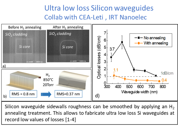
[1] C. Bellegarde, H. El Dirani, X. Le Tartre, C. Petit-Etienne, C. Monat, J.-M. Hartmann, C. Sciancalepore and E. Pargon “Technological advances on Si and Si3N4 low-losses waveguide platforms for nonlinear and quantum optics applications”, Proc. SPIE OPTO 10933, Advances in Photonics of Quantum Computing, Memory, and Communication XII, 1093309 (2019). doi: 10.1117/12.2508617
[2] H. El Dirani, F. Sabattoli, F. Garrisi, C. Petit-Etienne, J.-M. Hartmann, E. Pargon, C. Monat, M. Liscidini, M. Galli, D. Bajoni, C. Sciancalepore, "Low-Loss Silicon Technology for High-Q bright Quantum Sources", 2019 IEEE International conference on Group IV photonics (GFP), ThA: Advances in novel devices. doi:10.1109/group4.2019.8853895
[3] Q. Wilmart, C. Bellegarde, C. Petit-Etienne, L. Youssef, J-M Hartmann, D. Fowler, S. Brision, S. Garcia, A. Myko, K. Ribaud, P. Grosse, B. Charbonnier, S. Bernabé, C. Sciancalepore, E. Pargon, B. Szelag, Ultra low-loss silicon waveguides for 200 mm photonics platform, 2019 IEEE International conference on Group IV photonics (GFP), WC: Silicon Nitride Devices and Platforms, DOI: 10.1109/group4.2019.8853923
[4] Q. Wilmart, S. Brision , J-M Hartmann , A. Myko , K. Ribaud , C. Petit-Etienne , L. Youssef , D. Fowler , B. Charbonnier , C. Sciancalepore , E. Pargon , S. Bernabé , B. Szelag, “A complete Si photonics platform embedding ultra-low loss waveguides for O- and C-band”, Journal of Lightwave Technology 39, NO. 2, 532-538, (2021), Doi: 10.1109/JLT.2020.3030123.
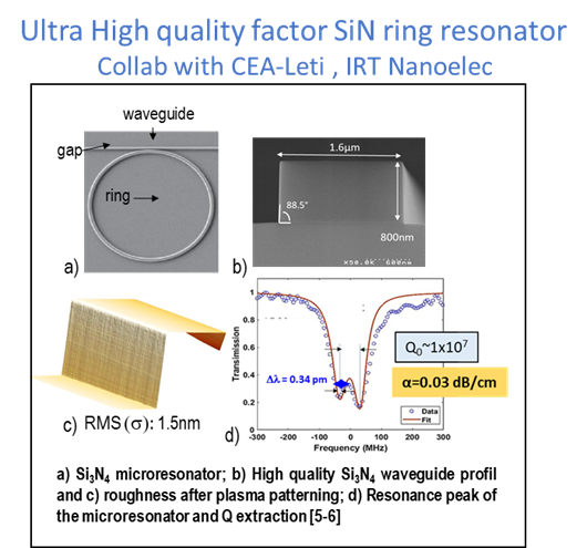
[5] H. El Dirani, F. Sabattoli, F. Garrisi, C. Petit-Etienne, J.-M. Hartmann, E. Pargon, C. Monat, M. Liscidini, M. Galli, D. Bajoni, C. Sciancalepore, "Low-Loss Silicon Technology for High-Q bright Quantum Sources”, 2019 IEEE International conference on Group IV photonics (GFP), ThA: Advances in novel devices. doi:10.1109/group4.2019.8853895
[6] Q. Wilmart, C. Bellegarde, C. Petit-Etienne, L. Youssef, J-M Hartmann, D. Fowler, S. Brision, S. Garcia, A. Myko, K. Ribaud, P. Grosse, B. Charbonnier, S. Bernabé, C. Sciancalepore, E. Pargon, B. Szelag, Ultra low-loss silicon waveguides for 200 mm photonics platform, 2019 IEEE International conference on Group IV photonics (GFP), WC: Silicon Nitride Devices and Platforms, doi: 10.1109/group4.2019.8853923
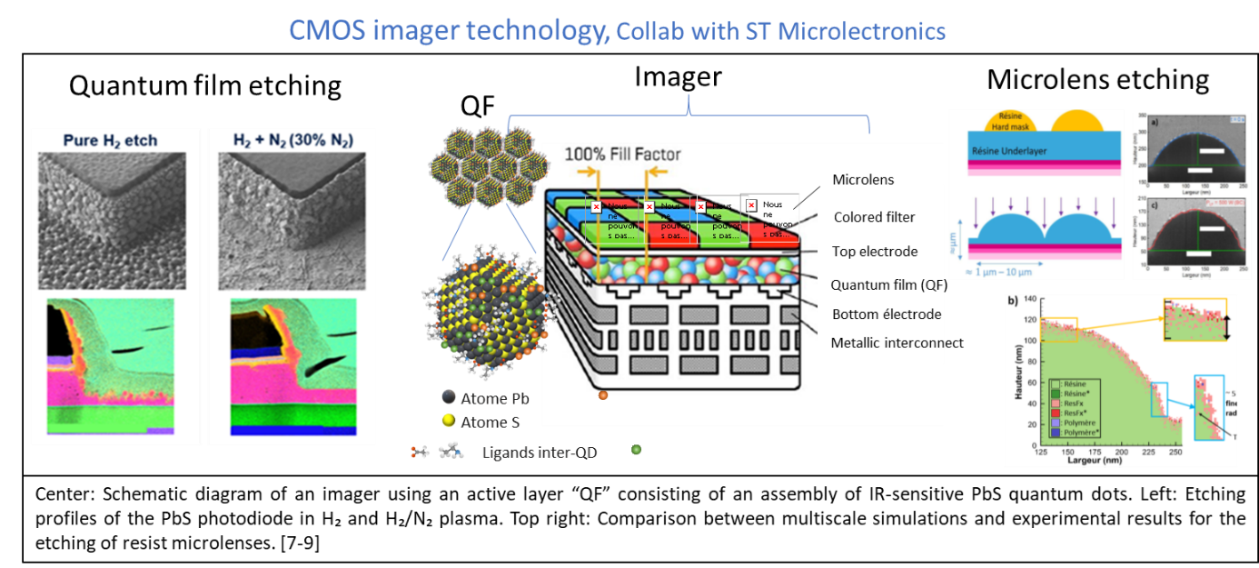
[7] P. Ducluzaux, D. Ristoiu, G. Cunge, E. Despiau-Pujo, “Impact of plasma operating conditions on the ion energy and angular distributions in dual-frequency capacitively coupled plasma reactors using CF4 chemistry” , J. Vac. Sci. Technol. A 42, 013002 (2024), https://doi.org/10.1116/6.0003291
[8] N. LE BRUN, G.CUNGE, P. GOURAUD, C. PETIT-ETIENNE, L.PARMIGIANI, S. ALLEGRET-MARET, D.GUIHEUX, J.S. STECKEL “PbS quantum dot thin film dry etching” ,J. Vac. Sci. Technol. A 42, 033007 (2024) https://doi.org/10.1116/6.0003335
[9] S. Younesy, C. Petit-etienne, S. Barnola, P. Gouraud, G. Cunge, “Cleaning chamber walls after ITO plasma etching process SPIE proceeding, advanced etch technology for nanopatterning IX, 11329, P.30 (2020) DOI: 10.1117/12.2549210
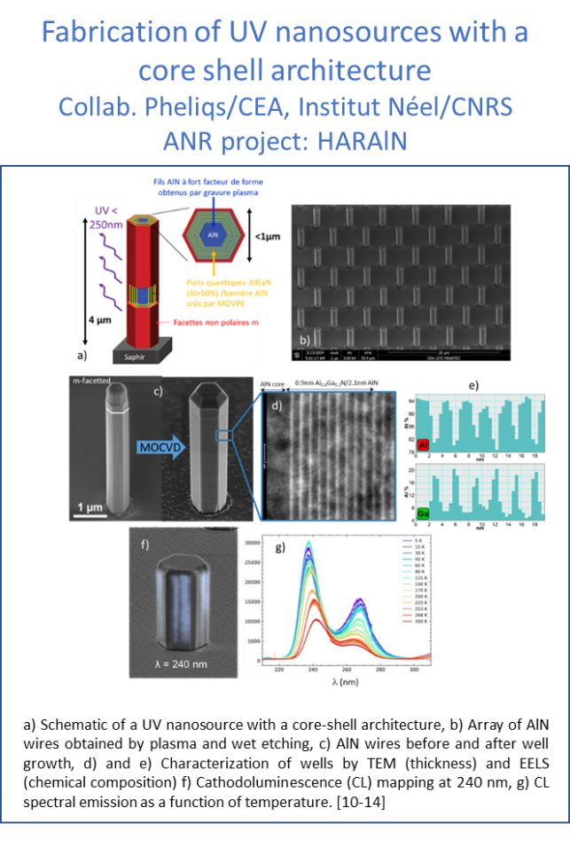
[10] L. Jaloustre , V. Ackermann , S. Sales De Mello Saron , S. Labau, C. Petit-Etienne, E. Pargon, « Preferential crystal orientation etching of GaN nanopillars in Cl2 plasma”, Mater. Sci. Semicond. Process. 165, 107654 (2023), Doi : 10.1016/j.mssp.2023.107654
[11] Lucas Jaloustre, Saron Sales De Mello, Sébastien Labau, Camille Petit-Etienne, Erwine Pargon, "Faceting mechanisms of GaN nanopillar under KOH wet etching”, Materials Science in Semiconductor Processing, Volume 173, 108095, (2024) doi : 10.1016/j.mssp.2023.108095
[12] Jaloustre Lucas, Sales De Mello Saron, Labau Sébastien, Petit-Etienne Camille, Pargon Erwine , "Fabrication of high aspect ratio AlN nanopillars by top-down approach combining plasma etching and wet etching”, Materials Science in Semiconductor Processing 18, 108615 (2024) doi: 10.1016/j.mssp.2024.108615
[13] Lucie Valera, Lucas Jaloustre, Valérie Reita, Saron R.S. De Mello, Edith Bellet-Amalric, Camille Petit-Étienne, Erwine Pargon, Gwénolé Jacopin, and Christophe Durand, “Organized AlN Nanowire Arrays by Hybrid Approach of Top-Down Processing and MOVPE Overgrowth for Deep UV Emission Devices”, ACS Appl. Nano Mater. 7, 9, 10338–10349, (2024), doi 10.1021/acsanm.4c00814
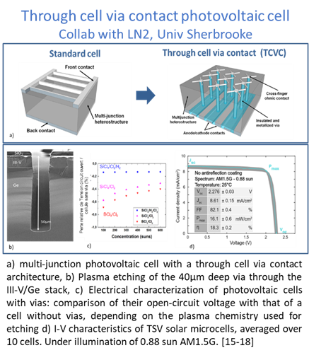
[14] M. De Lafontaine, E. Pargon, C. Petit-Etienne, G. Gay, A. Jaouad, M.-J. Gourb, M. Volatier, S. Fafard, V. Aimez, M. Darnon, “Influence of Plasma Process on III-V/Ge Multijunction Solar Cell Via Etching.” , Solar cells energy and materials 195, 49-54 (2019). Doi : 10.1016/j.solmat.2019.01.048
[15] M. de Lafontaine, E. Pargon, G. Gay, C. Petit-Etienne, S. David , J-P Barnes, N. Rochat, A. Jaouad, M. Volatier, S. Fafard, V. Aimez, M. Darnon, “Anisotropic and low damage III-V/Ge heterostructure etching for multijunction solar cell fabrication with passivated sidewalls”, Micro and nano engineering 11, 100083 (2021) DOI : 10.1016/j.mne.2021.100083
[16] M. de Lafontaine, G . Gay, E. Pargon, R. Stricher, S. Ecoffey, M. VolatierA. Jaouad, S. Fafard, V. Aimez, and M. Darnon, "III-V/Ge Multijunction Solar Cell with Through Cell Via Contact Fabrication and Characterization," 2021 IEEE 48th Photovoltaic Specialists Conference (PVSC), 20-25, pp. 2231-2233, (2021), doi: 10.1109/PVSC43889.2021.9519047.
[17] M. de Lafontaine, F. Ayari, E. Pargon, G. Gay, C. Petit-Etienne, A. Turala, G. Hamon, A. Jaouad, M. Volatier, S.Fafard, V. Aimez, M. Darnon “Multijunction solar cell mesa isolation: Correlation between process, morphology and cell performance”, Solar Energy Materials and Solar Cells 239, 111643 (2022), Doi : 10.1016/j.solmat.2022.111643
[18] M. de Lafontaine, T. Bidaud, G. Gay, E. Pargon, C. Petit-Etienne, A. Turala, R. Strichera, S. Ecoffey, M. Volatier, A. Jaouada, S. Fafard, V. Aimez, M. Darnon,” 3D Interconnects for III-V Semiconductor Heterostructures for Miniaturized Power Devices”, Cell Reports Physical Science 4, 101701, (2023) doi.org/10.1016/j.xcrp.2023.101701
- Share
- Share on Facebook
- Share on LinkedIn