- Share
- Share on Facebook
- Share on LinkedIn
2D materials are promising candidates for drastically reducing material usage in IoT applications, while offering properties equivalent to—or even superior to—their bulk counterparts at thicknesses of only a few nanometers. Despite their relatively recent emergence, their potential for electronic and optoelectronic devices is being actively explored, particularly with a view to integration on industrial platforms. However, numerous technological bottlenecks still hinder their large-scale implementation.
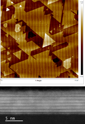
At LTM, our work focuses on the large-scale growth of 2D III–VI monochalcogenide materials, such as GaSe and InSe, their characterization, and the identification of applications compatible with CMOS processes. Their bandgaps vary with thickness: GaSe shifts from 2.0 eV (620 nm) to 3.5 eV (354 nm) in the monolayer, and InSe from 1.25 eV (992 nm) to 2.11 eV (588 nm). These variations cover a broad spectral range, from the near-IR to the UV, paving the way for multiband photodetectors. Today, these materials are mostly based on exfoliated layers and therefore require the development of processes compatible with large-scale manufacturing—precisely the objective of the project we are developing.
- Share
- Share on Facebook
- Share on LinkedIn