
Intership M2
- Share
- Share on Facebook
- Share on LinkedIn
Job description / Training
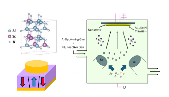
RESEARCH OPPORTUNITY:
The von Neumann electronic architecture is one of the main obstacles to low-energy artificial intelligence (AI): the separation between processing and memory cores induces major energy overconsumption. Neuromorphic electronics based on spiking neural networks and the computing-in-memory (CIM) paradigm paves the way for low-energy AI. In this landscape, capacitive CIM based on ferroelectric capacitive memories (memcapacitors) is emerging as an ultra-low-energy approach, free from the inherent limitations of resistive CIM based on memristors (leakage currents, voltage drops, high currents). The next-generation ferroelectric material AlScN is a promising candidate for high-performance memcapacitors, with a remanent polarization above 100 μC/cm² and a low-temperature PVD deposition process (<300 °C) requiring no crystallization annealing. This 6-month Master 2 internship proposes to develop sub-10 nm AlxSc1-xN ferroelectric films deposited by confocal PVD with an optimized stoichiometry for low-voltage ferroelectric switching, high remanent polarization and memcapacitive performance.
SCIENTIFIC CHALLENGES:
Within an ecosystem of experts, you will lead the following research activities:
• Development of a confocal PVD process: You will develop a dual-target magnetron co-sputtering process (AlN and Sc targets) on the new PLASSYS MP500S system acquired by LTM and installed at LMGP. You will control the stoichiometry of the films and achieve the sub-10 nm thicknesses required for low-voltage ferroelectric switching.
• Structural and chemical characterization: You will conduct a multi-technique investigation of the films: X-ray diffraction and reflectivity (XRD/XRR) to determine the crystal phase (ferroelectric wurtzite vs. cubic), density and thickness; X-ray photoelectron spectroscopy (XPS) to analyze chemical bonding states and stoichiometry; electron microscopy (SEM/TEM) with energy-dispersive X-ray spectroscopy (EDX) to assess grain morphology, interface quality, the Al/Sc ratio and homogeneity; Raman spectroscopy to identify local structural distortions and stresses.
• Electrical characterization of devices: In close collaboration with a PhD student at LTM, who will fabricate CMOS-compatible Metal-Ferroelectric-Metal (MFM) capacitors in LTM’s cleanroom facilities, you will contribute to PUND measurements (remanent polarization 2Pr, coercive field Ec), C-V measurements to evaluate the capacitive memory window, pulsed I-V sequences to demonstrate and optimize multi-level capacitance programming and non-destructive capacitive readout via transient currents, and cycling measurements to assess endurance and variability.
AN EXCEPTIONAL ENVIRONMENT IN EUROPE:
The internship will take place within the framework of the PEPR DIADEM, in a collaboration between the Laboratory of Technologies for Microelectronics (LTM) and the Laboratoire des Matériaux et du Génie Physique (LMGP, Grenoble INP), in the heart of Europe's largest R&D hub for nanotechnologies.
• Technology platforms: You will benefit from direct access to the new PLASSYS MP500S deposition system, and to the cleanroom and characterization facilities of the Upstream Technological Plateform (PTA) and CIME Nanotech.
• Network & collaborations: You will work in close collaboration with researchers at LTM and LMGP, and with a PhD student in cotutelle between Université Grenoble Alpes (UGA) and Université de Sherbrooke (UdeS).
• Excellence training: You will develop a unique profile combining thin-film growth, materials characterization and emerging memory devices for neuromorphic electronics. Results will be valorized through seminars and publications. A doctoral thesis may follow the internship, subject to funding.
Candidate profile:
Requires enrollment in a Master 2 program (or engineering school) in Materials Science or Nanotechnologies. You demonstrate a solid foundation in solid-state physics, microfabrication and materials science, with a particular interest in ferroelectric phenomena and thin-film technologies. Practical experience or strong theoretical knowledge of sputtering deposition processes and electrical characterization (C-V, I-V, DC and pulsed) is a significant asset. Strong analytical skills to interpret complex structural and chemical data, scientific rigor, autonomy, and the ability to work within a collaborative research environment involving multiple laboratories are required. Fluent technical English is required.
Starting date: February or March.
Application: Please submit your CV, transcripts from the last two years, and, if possible, letters of recommendation.
Contact: yann.beilliard univ-grenoble-alpes.fr (yann[dot]beilliard[at]univ-grenoble-alpes[dot]fr)
Supervisors: LTM: Yann Beilliard, LMGP: Eirini Sarigiannidou, Vincent Consonni
Download
offre M2 (PDF, 157.58 KB)
- Share
- Share on Facebook
- Share on LinkedIn