- Share
- Share on Facebook
- Share on LinkedIn
To meet these challenges, we have developed CMOS-compatible pathways to grow and integrate III-V semiconductors based on arsenic, phosphorus and antimony.
The choice to study and develop growth processes on standard microelectronics substrates, namely nominal Si(100) with a diameter of 300 mm, constitutes a major technological challenge. These materials can have applications in the fields of nanoelectronics, optoelectronics and sensors. This technological challenge comes from the fact that III-V materials and silicon present incompatibilities which complicate the crystal growth of the former on the latter. In order to make the most of the technological developments of recent decades, we have decided to work in a completely Si environment, that is to say the 300 mm CMOS clean room at CEA-LETI, in partnership with the equipment manufacturer number 1 in microelectronics Applied Materials.
We have obtained major results in this area by studying the growth of GaAs and GaSb.
We have developed a surface preparation process coupling plasma cleaning with annealing under dihydrogen which allows the formation of biatomic steps and thus eliminate crystal defects called antiphase walls on nominal Si(100) substrates.
We are the only group in the world to master this technology in a controlled and reproducible manner, without Si buffer growth or substrate structuring.
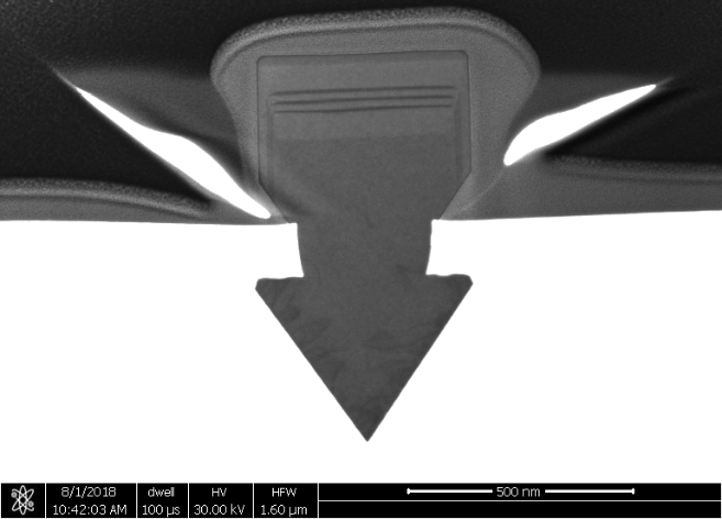
It thus becomes possible to obtain thin layers (140 nm) of GaAs epitaxied on silicon without antiphase walls (Thesis R. ALCOTTE, Thin Solid Films, 645, pp. 119-123 (2018)).
We recently demonstrated that this surface preparation also works for the growth of GaSb buffer layers on Si(100) since we obtained the same type of result, namely GaSb epitaxially grown on Si(100) 300 mm without a wall of antiphase (Thesis T. CERBA, Thin Solid Films, 645, pp. 5-9 (2018)).
Our objective is to produce components from these buffer layers and in particular laser structures (IRT NANOELEC Program).
In order to save time in this international competition with the University of Santa Barbara in particular, we have developed two major collaborations, one with University College London (UCL) to produce an arsenide-based laser emitting at 1.3µm telecom wavelength. , and the other with IES Montpellier to produce a laser based on antimonides emitting at 2.1 µm.
With UCL, we have produced the first electrically pumped laser operating continuously and emitting at 1.3 µm at room temperature (UCL and LTM publication in Optics Express 25(5), pp. 4632-4639 (2017)).
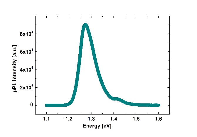
With IES, the first results are very encouraging since a laser emission at 2.3 µm was obtained by optical pumping at the temperature of liquid nitrogen.
This work was carried out as part of a joint development project (2012-2019) between the CNRS-LTM, the CEA-LETI and the company Applied Materials, number 1 equipment manufacturer for microelectronics based in Santa Clara (USA) on this subject, from the European H2020 COMPOSE3 program, Labex MINOS, the IDEX “NEED for IoT” project and IRT NANOELEC.
- Share
- Share on Facebook
- Share on LinkedIn