- Share
- Share on Facebook
- Share on LinkedIn
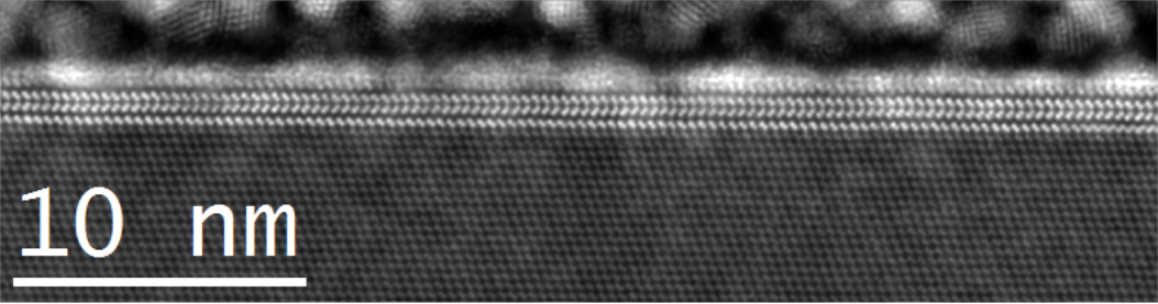
In order to further reduce the consumption of gallium and indium, we launched a new theme in 2017 on the hetero-epitaxy of 2D type III-VI materials. There is a significant zoology of 2D materials based on selenium, sulfur or tellurium (chalcogenides) exhibiting semiconductor properties. The most currently studied “post-graphene” materials are probably the transition element dichalcogenides (TMDCs): MoSe2, MoS2 and WSe2… These materials have remarkable properties (optics, spintronics, valleytronics, etc.) when they are placed in the form of a monolayer. In recent years, there has been growing interest in a new class of 2D materials, III-VI materials. Unlike TMDCs, these materials have interesting properties even on the scale of several monolayers: high mobility, strong second harmonic generation, low exciton binding energy, direct band structure, etc. Among these materials, the (Ga-) family In) Se has shown strong potential for applications in nanoelectronics, optoelectronics, nonlinear optics, fast response photodetectors, terahertz sources. This subject is new and prospective, and we are working to develop large-scale processes (200 and 300 mm) for the hetero-epitaxy of single-crystal layers of GaSe and InSe on Si (100) and Si (111). Indeed, there is currently no method that allows these 2D materials to be produced on an industrial scale in terms of processes, substrate size, production yield and precise positioning of the materials on the wafer. Drawing on our experience on the hetero-epitaxy of III-V/Si, we have chosen MOCVD on standard Si (100) 300 mm and Si (111) 200 mm microelectronic substrates used in the GaN/Si sector in 200mm.
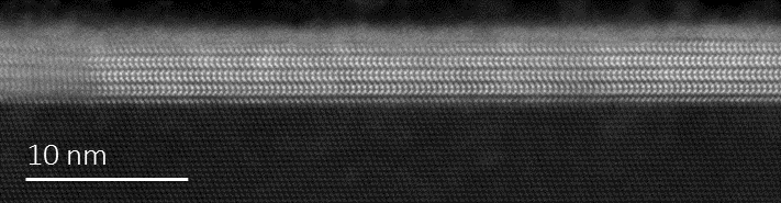
As a first step, we therefore integrated a selenium source into our MOCVD 300 mm industrial III-V semiconductor epitaxy reactor. Our objective is to study and develop a rupture process allowing the manufacture of GaSe and InSe layers by Van der Waals epitaxy from commercial organometallic precursors (trimethylgallium and Diisopropyselenide). The preparation of the Si surface before deposition is derived from that developed for direct epitaxy of III-V/Si semiconductors; this preparation seems universal and well suited for heteroepitaxy on Si. The use of the Si (111) 200 mm substrate allowed us to obtain monolayers of GaSe and InSe presenting a unique crystalline orientation and grain sizes of the order of 1 to 5 µm. Emission at 630 nm was obtained by photoluminescence at room temperature.
- Share
- Share on Facebook
- Share on LinkedIn