- Share
- Share on Facebook
- Share on LinkedIn
Di-block copolymers are currently considered as a possible new generation lithography in microelectronics due to their high resolution.
They are composed of two blocks (polymer chains) linked by a covalent bond. Depending on the molecular weight of each block, their relative volumes and the chemical incompatibility between each block (measured by the Flury-Huggins factor χ), it is possible to form periodic structures from these materials by separation of micro-phases.
In the literature, the most used copolymer is polystyrene-b-polymethylmethacrylate (PS-b-PMMA) due to its ease of implementation, but these are so-called “high χ” materials which are necessary to go down to high resolutions. less than 10 nm, an area of greatest interest to microelectronics manufacturers.
The LTM is particularly interested in the implementation, self-assembly and etching of these so-called “high χ” materials, and particularly in recent years in those with a lamellar morphology, which are more promising for applications of very resolved and dense lines in microelectronics (interest for transistor architectures such as FinFETs in particular).
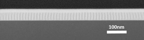
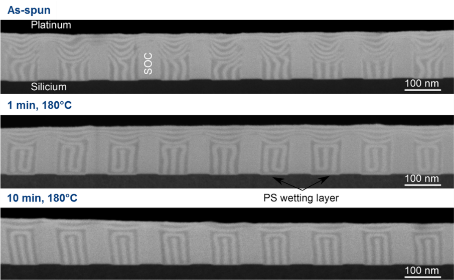
Thanks to two European projects and a French project in progress (coordinated by Arkema) and thanks to the presence of an Arkema engineer and technician in the laboratory, we have worked on polymers and neutralization layers (necessary at the top and at the bottom of the block copolymer layer to orient the lamellae perpendicular to the substrate) synthesized by this manufacturer. We chose to deepen the work on a particular polymer: PS-b-Poly (1,1-dimethyl silacyclobutane) (PDMSB). As shown in Figure 4 (bottom), using lines of organic resin, we were able to obtain perpendicular lamellae of 100 nm height with a polymer with a period of 23 nm, this on large areas (~cm2), according to a technique called “graphoepitaxy” (use of surface topography to guide organization). Furthermore, the work on the neutralization layers made it possible to demonstrate the organization of a lamellar polymer with a period of 14 nm (7 nm resolution) perpendicular to the substrate without guide lines.
The continuation of the work is the extension of these approaches to substrates up to 300 mm in diameter as well as the control of long-distance order by “chemo-epitaxy” by creating a chemical structuring of the surface.
- Share
- Share on Facebook
- Share on LinkedIn