- Share
- Share on Facebook
- Share on LinkedIn
After developing various nanoimprinting techniques for years, over the past 5 years we have expanded our expertise by optimizing complete nanofabrication processes for particular applications, most of these processes using a nanoprinting step.
We can distinguish these process/application pairs according to two main criteria:
if we consider the technological aspect, many of our activities in recent years have consisted of developing structuring processes on flexible substrates such as polymer sheets.
But we continued to optimize processes on silicon or glass, with or without nanoprinting step.
If we consider our activities from the perspective of applications, a certain number of them concern the field of optics, but also other sectors such as applications of superhydrophobic surfaces [Durret Applied Surface Science 2018], solar cells [Reynaud Journal of Nanoparticle Research 2017] or SERS substrates [Ferchich, Microelectronic Engineering 2015].
We cannot detail them all in this report and we will focus on three of them.

- Nanoimprinting is of major interest for the field of optical components.
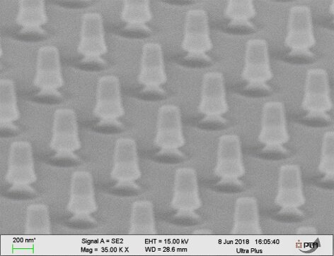
An example is the production of LEDs based on GaN on Si by pendeo-epitaxy. We have developed in collaboration with the CEA/LETI/DOPT as part of a Carnot project a manufacturing process for deformable SiO2 pillars which allow, during the regrowth of GaN, to significantly reduce the rate of dislocations by optimizing the the coalescence of raw GaN pyramids on these pillars (figure 2). The optimization of all the steps, including the definition of structures by nanoimprinting, makes it possible to ultimately envisage an industrial process.
- As part of a collaboration with the Institute of Planetology and Astrophysics of Grenoble and the European H2020 SCARBO program: Space CARBon Observatory
- Share
- Share on Facebook
- Share on LinkedIn