- Share
- Share on Facebook
- Share on LinkedIn
A promising way to improve the performance of integrated circuits is 3D integration which consists of stacking chips on top of each other (heterogeneous 3D) or superimposing MOSFET transistors or tunnel effect transistors one on top of the other on the same chip (monolithic 3D). This will increase the performance of integrated circuits by adding new functionalities.
Two major routes are used to create 3D circuits, which are mainly the transfer of chips and the direct manufacturing of transistors on top of each other without going through the bonding stage.
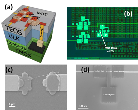
The monolithic approach requires a thermal budget limited to 450 °C in order not to degrade the performance of the “Front End Of Line” MOSFET transistors. In this context, we have, first of all, succeeded in showing, for the first time, a proof of concept of a guided growth, between two metal electrodes, of horizontal nanowires directly on a silicon substrate covered by an oxide. To do this, we optimized the growth parameters of SiGe nanowires at low temperature and then between predefined electrodes, we succeeded in confining this growth inside the oxide trenches thanks to the “nanodamascene” process [M. MERHEJ et al., Microelectronic Engineering, 177, pp. 41-45, (2017)]. The location of the catalysts was the key point of this process to control and eliminate the random growth of horizontal nanowires.
Secondly, we developed a new technological process based on the dielectrophoresis technique to produce nanowire channel transistors connected to CMOS logic (CMOS chip from ST Microelectronics). First, we made the vias to connect the MOSFET transistors to our upper contacts. Then we optimized the key parameters of dielectrophoresis and finally we produced the horizontal nanowire channel transistor [M. MERHEJ et al., Semiconductor Science and Technology, 33 (1), art. no. 015005, (2018)]. The electrical characteristics of these devices connected to CMOS logic are very encouraging. This research work is carried out as part of Mr. Merhej's thesis in collaboration with LN2 in Sherbrooke (2013-2017).
- Share
- Share on Facebook
- Share on LinkedIn