- Share
- Share on Facebook
- Share on LinkedIn
The increase in the performance of integrated circuits due to the miniaturization of the MOSFET will face a technological and scientific wall in a few years.
One of the issues is the increase in static and dynamic power in integrated circuits. In order to reduce this power consumption, new architectures and new materials which will make it possible to obtain a low operating voltage (VDD) are today intensively studied.
Tun-FET transistors, whose channel consists of a thin film or a nanowire with heterojunctions, are considered promising candidates to replace or complement current MOSFET-based technology. In addition, the geometry of the nanowires makes it possible to obtain an almost ideal structure from an electrostatic point of view, with the possibility of 3D integration.
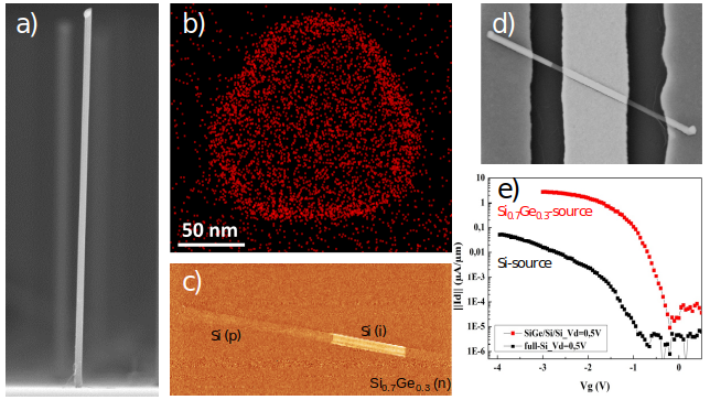
In this context, we are interested in the optimization of the growth parameters (temperature, ratio of partial pressure of precursors) for the fabrication of IV-IV nanowires containing axial heterostructures (Si, SiGe, GeSn) and/or doping heterojunctions (n-type using PH3 and p-type with B2H6).
These nanowires with axial heterostructures are subsequently integrated into horizontal Omega gate transistors to measure their electrical characteristics. The growth of the nanowires is carried out by CVD (chemical deposition) assisted with different metallic catalysts, mainly Au using the VLS (vapor-liquid-solid) mechanism [V. BROUZET et al., Applied Physics A, Volume 121, Issue 3, Pages 1285-1290, (2015)].
The physicochemical properties of the nanowires such as the morphology, the stiffness of the interfaces, the spatial distribution of the chemical elements as well as the chemical concentration of the alloys are determined by SEM, HAADF-STEM and/or EDX-STEM, Auger electron spectroscopy under Argon abrasion, RAMAN measurements and SCM measurements.
Recently, we have focused our efforts on the growth of nanowires based on the GeSn alloy which presents a direct gap for Sn concentrations above 8% and also a low gap (< 0.66 eV at 300 K) interesting as a source material in order to increase the ON current of the transistor and obtain electrical characteristics with a steep subthreshold slope for the production of low consumption devices. Auger and STEM-EDX measurements showed us a radial distribution of Sn in GeSn nanowires with a core-shell structure with Sn enrichment on the nanowire surface (> 10%) [T. HAFFNER et al., Phys. Status Solidi A Volume 215, 1700743, 2018]. This work was carried out as part of the IDEX-Labex MINOS project.
- Share
- Share on Facebook
- Share on LinkedIn