- Share
- Share on Facebook
- Share on LinkedIn
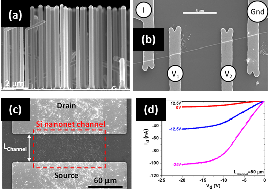
Following the 3D integration and within the framework of the H2020 “nanonets2sense” project, the main objective is to create a low-cost generic biosensor based on Si nanowires, interconnected to CMOS logic, with better sensitivity than current biosensors.
To achieve this objective and thanks to our expertise in the field of integrating nanowires into FET-type devices, we have removed several technological obstacles in order to improve the performance of such a device. The technological obstacles are:
(i) controlling the size and doping of the nanowires (length, diameter and doping level),
(ii) optimizing the contact resistance between the nanowire mat and the contact metal while respecting the constraint already mentioned which is the thermal budget,
(iii) the right choice of gate metal in order to properly adjust the threshold voltage [M. LEGALLAIS et al., Solid-State Electronics, 143, pp. 97-102, (2018)]. This work is carried out in close collaboration with IMEP-LAHC and LMGP in Grenoble and AMS in Austria, KTH in Sweden and Cambridge CMOS Sensors in the United Kingdom.
- Share
- Share on Facebook
- Share on LinkedIn