- Share
- Share on Facebook
- Share on LinkedIn
The aim of the ANR PEGADIS project is to develop a new type of GaN-based µLeds with optimized performance by growing GaN on deformable GaN/AlN/Si/SiO2-based pillar arrays. The benefits are linked to a bottom-up approach for pixel definition and a reduction in the dislocation density of GaN.

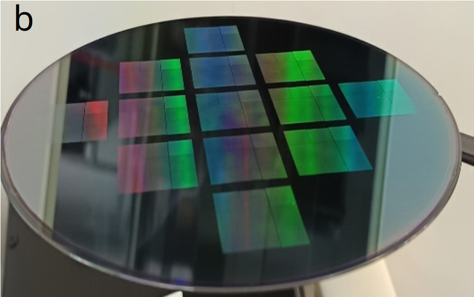
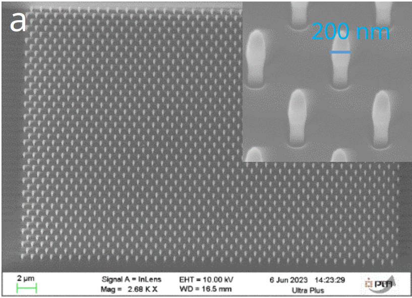
In addition to LTM, this project involves CEA LTI, CRHEA and CEMEF. LTM's role was to develop a complete integrative process on a 200 mm wafer, from the definition of nanopillars using nanoimprint to the etching of nanostructure arrays with virtually zero defectivity at wafer scale.

It is also important to control the verticality of the pillars on all etched layers. Optimization of each process step has led to defect-free arrays, as shown in the figure above.
- Share
- Share on Facebook
- Share on LinkedIn