- Share
- Share on Facebook
- Share on LinkedIn
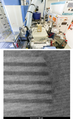
The use of III–V semiconductors, thanks to their physical properties, is particularly well-suited for the development of optical emitters and sensors operating in the infrared domain. We focus in particular on (Al, In, Ga)(As, P, Sb) alloys. To build a photonic integrated circuit (PIC), it is necessary to integrate different functions on a Si CMOS platform, including both the light source and the photodetector. Two approaches are possible: bonding or direct growth of III–V materials on silicon. Bonding is currently the most common technique and is used in foundries to integrate on-chip lasers (Intel or Luxtera). The GaAs or InP substrate serves only as a support and is then removed, which is problematic given the criticality of Ga and In elements. Monolithic integration, also called direct growth on silicon, is a technique under active development. Direct heteroepitaxy of III–V materials on silicon generates structural defects that degrade device performance. We have shown that it is possible to mitigate defects associated with thermal expansion coefficient and polarity mismatches. Nevertheless, the lattice parameter mismatch between Si and GaAs and its alloys inevitably leads to the formation of dislocations that propagate into the layers and active regions.
We are also working on a breakthrough technology to integrate high-frequency III–V transistors within a 200/300 mm silicon manufacturing environment, addressing the requirements of future 6G wireless systems. This involves developing, ex nihilo, a process flow compatible with silicon’s industrial constraints, enabling the cohabitation of III–V and Si worlds on the same substrate. LTM is at the heart of this innovation, with the development of double heterojunction bipolar transistors (DHBTs) based on InP/GaAsSb junctions—an original and promising alternative to conventional architectures—which will ultimately be implemented on 200 mm InPoSi (InP-on-Si) substrates.
- Share
- Share on Facebook
- Share on LinkedIn