
Internship Master II
- Share
- Share on Facebook
- Share on LinkedIn
Job description / Training
Key words: nanophotonics, biodiversity, photonic nanostructure properties, microcavities, electromagnetic simulations
Context
Semiconductor nanophotonics exploits nanoscale structuration of materials to manipulate light at dimensions smaller than its wavelength, enabling ultra-compact, high-efficiency photonic devices. It can combine quantum effects (e.g., quantum dots) and nanostructures (e.g., photonic crystals, waveguides) for light emission, modulation, and detection. Thanks to microelectronics-derived technologies, photonic systems are produced with high fabrication precision, achieving layered mirror structures that reflect specific wavelengths via constructive interference or extreme optical performance — such as high-Q microcavities (Fig.A).
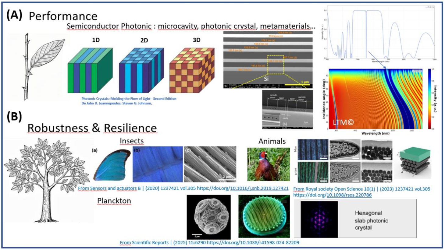
Figure: (A) Semi-conductor based nanophotonic, SEM and modelisation of optical microcavity (B) Photonic properties of plankton, insects and animals
Nature has also evolved living systems that, through the structuring of organic materials, achieve nanophotonic systems near to photonic crystals (Fig.B). These structures selectively reflect specific wavelengths, enhancing camouflage or signaling.
The robustness of those self-assembly living system that maintain their function and integrity in the face of internal/external perturbations inspire biomimetic applications. This internship will focus on the fine optical study of living systems exhibiting nanostructures, with connections to the field of semiconductors
Internship objectives
The student will combine morphological analysis (SEM/TEM), angular reflectance spectroscopy observations and electromagnetic simulations (TMM, Plane-Wave etc..) to characterize insects/animals optical properties for color structuration.
He will study how the contribution of biological photonic nanostructures based on evolutionary-optimized solutions for durability, broadband reflection, and angle-independent color can inspirate semiconductor nanophotonic. He will participate to build a localized angle/polarization resolved spectral micro-reflectometer for microorganisms optical analysis.
Scientific and Technological Environment
The internship will be carried out mainly at the Microelectronics Technologies Laboratory located on the CEA-LETI-MINATEC site.
A PhD opportunity in this research area is being considered
Skills
We are looking for a motivated Master 2 student in nanophysics, who understands the physical principles of nanooptics, has skills in programming (Python) and enjoys building experiment. The candidate should also have good communication skills in both French and English, as well as the ability to clearly report and present their work. They should enjoy working as part of a team while demonstrating autonomy, dynamism, and rigor.
Practical information
- Level: Master 2 internship
- Duration: 6 months
- Starting date: 2027
- Compensation:
Contact
Dr. PEYRADE David
david.peyrade cea.fr (david[dot]peyrade[at]cea[dot]fr)
tel: 04 38 78 24 53
- Share
- Share on Facebook
- Share on LinkedIn