
Intership M2
- Share
- Share on Facebook
- Share on LinkedIn
Job description / Training
Key words: Plasma etching processes, pulsed plasmas, amorphous carbon, block copolymer
Context
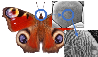
Mastering the structuring of matter at the nanoscale now makes it possible to design surfaces with novel properties. In optics, hierarchical surfaces inspired by natural structures, such as butterfly eyes, can improve light transmission, reduce reflections, and even provide self-cleaning properties.
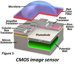
This internship is part of the development of a novel approach to nanostructuring the surfaces of microlenses integrated into a CMOS sensor, which is the subject of a patent. The main bottleneck of the integration is the transfer of nanoscale patterns, with feature sizes of a few tens of nanometers, obtained by block copolymer lithography, into amorphous carbon layers several micrometers thick. This represents a considerable challenge: achieving structures with aspect ratios greater than 30 while maintaining highly anisotropic profiles.
To address this challenge, the project explores an innovative approach based on pulsed plasmas. Temporal plasma modulation provides better control over the fluxes of chemical and physical species involved in etching, thereby enabling patterning regimes that are difficult or even impossible to achieve using conventional processes.
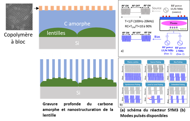
The objective of this Master's project is to develop pulsed plasma etching processes for producing high-aspect-ratio structures in amorphous carbon using block copolymer lithography. Successful completion of this project would represent the first step towards the full integration of nanostructured microlens surfaces into CMOS image sensors.
Internship objectives
The objective of the internship will be to demonstrate the potential of pulsed plasmas for fabricating nanostructures with very high aspect ratios. The work will combine:
- Investigation of the etching mechanisms of amorphous carbon;
- Optimization of plasma conditions and selectivity with respect to the lithographic mask;
- Transfer of nanoscale patterns into carbon layers several micrometers thick;
- Characterization of the resulting structures using SEM/FIB-SEM;
- Investigation of the underlying physical and chemical mechanisms using various plasma and surface diagnostics (optical emission spectroscopy, ion flux and energy measurements, XPS, AFM).
The candidate will therefore have the opportunity to approach the project from both a technological and scientific perspective, depending on their interests, while maintaining a central objective: the fabrication of nanostructures with very high aspect ratios.
Beyond the targeted application, understanding the mechanisms governing very-high-aspect-ratio etching of amorphous carbon could find applications in advanced microelectronics technologies, particularly for 3D memory architectures.
Scientific and Technological Environment
Experiments will be carried out on a state-of-the-art industrial 300 mm inductively coupled plasma (ICP) reactor (SYM3, Applied Materials), equipped with pulsed power supplies and located in the cleanrooms of CEA/Leti in Grenoble.
The internship will take place within the LTM/CNRS laboratory, located at the CEA/Leti site in Grenoble, in close collaboration with the CEA/Leti teams who developed the patented technology.
A PhD opportunity in this research area is being considered, with funding currently being sought.
Skills
The candidate should have a strong interest in experimental work. Knowledge of plasma physics, cleanroom micro- and nanofabrication processes, particularly plasma etching, as well as material characterization techniques (ellipsometry, electron microscopy, XPS), would be valuable for successfully carrying out the internship. The candidate should also have good communication skills in both French and English, as well as the ability to clearly report and present their work. They should enjoy working as part of a team while demonstrating autonomy, dynamism, and rigor.
At the end of the internship, the candidate will have gained a solid foundation in patterning technologies, with a particular focus on advanced plasma etching processes.
Practical information
- Level: Master 2 internship
- Duration: 6 months
- Starting date: February/March 2027
- Compensation: €680/month
How to Apply ?
Please send your CV and your Master 1 and Master 2 transcripts to:
erwine.pargon cea.fr (erwine[dot]pargon[at]cea[dot]fr)
nicolas.possemecea.fr (nicolas[dot]posseme[at]cea[dot]fr)
Download
microlentilles-stage 2027-LTM.pdf (PDF, 845.97 KB)
microlentilles-stage 2027-LTM-english.pdf (PDF, 829.3 KB)
- Share
- Share on Facebook
- Share on LinkedIn