The team is developping innovative plasma etching and deposition processes with the objective to meet the technological needs of emerging nano- and opto-electronic devices.
To this end, we study the basic mechanisms involved in plasma processes by combining plasma analyses, process simulation/modelling and characterization of plasma/surface interactions. The strength of our research lies in the ability to develop plasma processes on 200-300mm substrates in state-of-the-art industrial etching reactors. All the process breakthroughs are directly transferable to our industrial partners (STMicroelectronics, AMAT).
This research gathers the activity of 7 CNRS/UGA permanents:
- BONVALOT Marceline (MC, UGA)
- CUNGE Gilles (DR, CNRS)
- DESPIAU-PUJO Emilie (MC, UGA)
- JOUBERT Olivier (DR, CNRS)
- KOGELSCHATZ Martin (MC, INP)
- PARGON Erwine (DR, CNRS)
- PETIT-ETIENNE Camille (IR, CNRS)
Five main topics of research are conducted to face the challenges related to the patterning and elaboration of complex stack of materials using state-of-the-art plasma etchers and deposition tools:
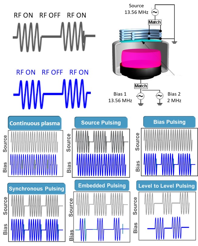
Advanced plasma technologies
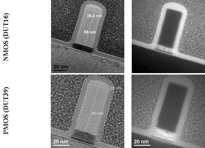
Advanced plasma Etching processes
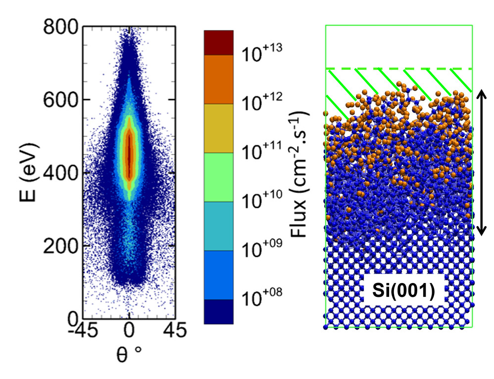
Plasma/surface modeling
Contact: emilie.despiau-pujo univ-grenoble-alpes.fr (emilie[dot]despiau-pujo[at]univ-grenoble-alpes[dot]fr)
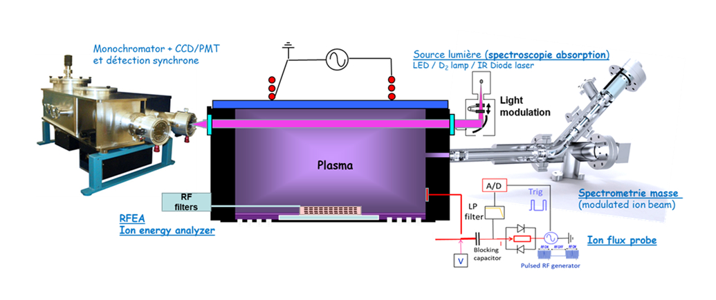
Plasma diagnostics
Plasma enhanced atomic layer deposition processes
Contact: marceline.bonvalot cea.fr (marceline[dot]bonvalot[at]cea[dot]fr)
