- Share
- Share on Facebook
- Share on LinkedIn
At the same time, the entire team participated in the development of Smart etch technology applied to the etching of the SiN spacers of FDSOI transistors. The modification of the material by implantation was characterized as a function of the flow and the energy of the ions, highlighting the important role of the implantation time (in agreement with MD) and our ability to modify the SiN material over 0.5 nm at 9 nm depth in a controlled manner. Then the etching mechanism of this layer in downstream plasma was analyzed.
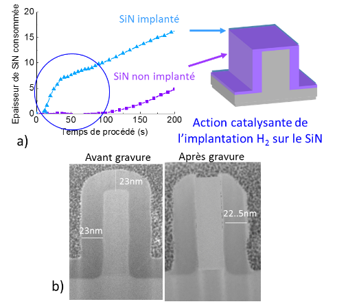
The key step was the development of a downstream NF3/NH3 plasma process selective between modified and unmodified material. These processes are very sensitive to surface conditions: there is an incubation time during which plasma radicals adsorb but no etching occurs. This time being significantly shorter on the material modified by H2 implantation (catalysis), we are able to obtain infinite etching selectivities between implanted and non-implemented SiN (see Figure). This is the most efficient existing process today for etching the SiN spacers of FDSOI transistors, the concept being generalizable to all types of materials and for applications other than microelectronics.
- Share
- Share on Facebook
- Share on LinkedIn